Semiconductor Materials and Nanostructures
Equipment
-
MOCVD reactors
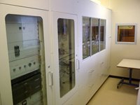 The group has one reactor dedicated to research & development of III-V semiconductors and a second reactor which is dedicated to II-VI compounds. The III-V system operates at atmospheric pressure, while the II-VI system is operated at low pressure. The horizontal quartz reactor tubes allow deposition of high homogenity thin films on substrates up to 2 cm2. Ultrapure hydrogen (III-V system) or argon (II-VI system) is used as carrier gas, and growth typically occurs between 400 and 700 °C. Our reactors are equipped with the following sources:
Materials and Structures:
The new MOCVD reactor has 6 lines, for of which are used for source precursors (gallium, indium, arsenic and antimony) while the other 2 lines are for an n-type (tin) and p-type dopant (cadmium or zinc). Several lines contain vapour flux monitors for accurate control of the source vapour delivery to the reactor, all mass flows are fully digital and signals are carried by optical fiber. All these features contribute to the controlled deposition of ultra-thin films and nano-sized structures in a reproducible way.
-
Hydrides: III-V: Arsine (AsH3); II-VI: tert-butanol
-
Organometallics: III-V: trimethylgallium, triethylgallium, trimethylindium ((CH3)3In), TMSb, TBAs, TESn; II-VI: diethylzinc
-
n-dopant: tetraethyl tin
-
p-dopant: dimethylzinc; dimethylcadmium
-
III-V semiconductor films such as: GaAs, InAs, InGaAs, InSb, GaSb, InAsSb, GaInSb with different composition and doping;
-
Nanostructures: Multi-quantum well (MQW) and superlattice (SL) structures; Nanorods; Quantum Dots (QD)
-
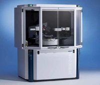
Scanning probe microscope
 The Bruker Dimension FastScan is the first atomic force microscope that combines high speed, ultra high resolution (sub-nanometer height), high precision, ultra-low drift and low noise. Its high bandwidth enables exceptional force control and high scan rates (as little as 1 sec per image frame). It incorporates all the advantages of the Dimension Icon (up to 30 modes of operation, high resolution and accuracy) but works 100s of times faster, improving productivity many-fold. The wide range of scanning modes available with this SPM make it ideally suited for the characterization of solids (conductive and insulating), fluids amd polymers in a range of disciplines spanning many of the branches in Biological, Physical and Chemical sciences.
More info and booking request
-
Variable temperature Photoluminescence system
Radiative recombination in a semiconductor gives invaluable information to the crystal grower about the overall quality of a film or nanostructure and provides information on the defect/impurity levels within the band gap. For studies of optical processes in the films produced in our laboratories, the department has two photoluminescence systems. The one system is dedicated to measurements between 350 nm and 1700 nm, using either an appropriate photomultiplier tube or a Ge detector coupled to a monochromator, while the other system is based on a Michelson interferometer for measurements between 2000 nm (2 mm) and 5000 nm (5 mm). Both systems are equipped with closed cycle He cryostats, capable of liquid He temperatures. The laboratory has three lasers for excitation: a 5 watt Ar-ion laser (with various lines between 457 and 514 nm), a 40 mW HeCd laser (325 nm line), and a 200 mW frequency doubled Nd:YAG laser (532 nm). Various visible and near-infrared laser diodes are also available for exciting the luminescence. A commercial "mini PL" system (from Photon Systems Inc), equipped with a NeCu laser (248 nm) allows measurements (room temperature to 77 K) on large band gap semiconductors emitting in the UV below 300 nm. Our PL laboratory is supported financially by the SA National Laser Centre.
-
X-ray diffraction
 X-Ray diffraction is based on the interaction between crystal structure of a material, and an x-ray beam having a wavelength similar in size to the spacing between the crystal planes. Under certain circumstances, x-rays scattered from different crystal planes in the sample will be in phase, and will constructively add to produce an intensity peak. The detection of these intensity peaks, and analysis of the conditions under which they occur, can give information about material composition and the quality of the material. The department has a state-of-the-art Bruker D8 Discover diffractometer, suitable for thin film and nanostructure characterization.
-
DLTS
DLTS stands for Deep Level Transient Spectroscopy. Using DLTS measurements, carriers are introduced in the sample under investigation using a bias pulse, changing the electron/hole occupation of a trap (crystal defect) in the semiconductor material. The measured junction capacitance of a metal - semiconductor contact increases as the electron occupation of the trap increases. DLTS is used to measure the activation energy (which is approximately the energy distance from the conduction or the valance band to the trap level) and the trap concentration in the MOCVD grown layers.
-
Raman spectroscopy
Raman spectroscopy is a spectroscopic technique used to study vibrational, rotational, and other low-frequency modes in a system. It relies on inelastic scattering also called Raman scattering of monochromatic light, usually from a laser in the visible, near infrared or near ultravilolet part of the spectrum. The laser light interacts with phonons or other excitations in the system, resulting in the energy of the laser photons being shifted up or down. Typically, a sample is illuminated with a laser beam. Light from the illuminated spot is collected with a lens and sent through a monochromator. Wavelengths close to the laser line, due to elastic Rayleigh sccattering, are filtered out while the rest of the collected light is dispersed onto a detector. As such, Raman spectroscopy provides useful information regarding defects and complexes present in the material under study.
-
Hydrogen plasma chamber
The department has a home-built dc plasma system for the creation of plasmas from hydrogen gas, nitric oxide, nitrogen, etc. The plasma is created between two biased electrodes. The density of the plasma can be qualitatitively controlled by varying the gas flow rate and the electric field between the electrodes. Sample temperatures of up to 600 °C are possible. Hydrogen and nitrogen are common impurities in semiconductors and this is a cheap and simple way to introduce these impurities and study their influence on the electrical and optical properties of a semiconductor.